-
产品详情
-
联系我们
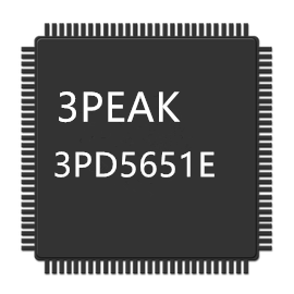
The 3PD5651E offers exceptional AC and DC performance whilesupporting update rates up to 125 MSPS. The 3PD5651E’s flexiblesingle-supply operating range of +2.7V to +5.5V and low power dissipation are well suited for portable and low power applications. Itspower dissipation can be further reduced to 45mW, without asignificant degradation in performance, by lowering the full-scalecurrent output. In addition, a power-down mode reduces the standbypower dissipation to approximately 20mW.The 3PD5651E is manufactured on an advanced CMOS process. Asegmented current source architecture is combined with a proprietaryswitching technique to reduce spurious components and enhancedynamic performance. Edge-triggered input latches and atemperature compensated bandgap reference have been integratedto provide a complete monolithic DAC solution. Flexible supplyoptions support +3V and +5V CMOS logic families.The 3PD5651E is a current-output DAC with a nominal full-scaleoutput current of 20mA and > 100kΩ output impedance.Differential current outputs are provided to support single-ended ordifferential applications. The current outputs may be directly tied to anoutput resistor to provide two complementary, single-ended voltageoutputs. The output voltage compliance range is 1.25V.The 3PD5651E contains a 1.10V on-chip reference and referencecontrol amplifier, which allows the full-scale output current to besimply set by a single resistor. The 3PD5651E can be driven by avariety of external reference voltages.The 3PD5651E’s full-scale current can be adjusted over a 2mA to20mA range without any degradation in dynamic performance. Thus,the 3PD5651E may operate at reduced power levels or be adjustedover a 20dB range to provide additional gain ranging capabilities.The 3PD5651E is available in 28-Lead TSSOP package. It isspecified for operation over the industrial temperature range.
FEATURES
⚫ 125 MSPS Update Rate
⚫ 10-Bit Resolution
⚫ Differential Current Outputs: 2 mA to 20 mA
⚫ SFDR at 100MHz clock with 1MHz output: 64 dBc
⚫ Fast Settling: 35 ns Full-Scale Settling to 0.1%
⚫ On-Chip 1.10 V Reference
⚫ Edge-Triggered Latches
⚫ Power Dissipation: 115 mW @ 5 V
⚫ Single +5 V or +3 V Supply Operation
⚫ Green, 28-Lead TSSOP Package
APPLICATIONS
⚫ Communications Transmit Channel
⚫ Signal Reconstruction
⚫ Direct Digital Synthesis (DDS)
⚫ Instrumentation
⚫ Video Reconstruction


